
Samsung Electronics has been a major player in the semiconductor industry since the early ‘80s and has strived to deliver advanced technologies that bring meaningful changes to our daily lives. In this report we will take a closer look at our semiconductor operations in Giheung and Hwaseong in Korea.
Trends in Semiconductor industry
Samsung’ Semiconductor Business has recently seen unprecedented success, largely owing to surging demand in advanced memory products for both consumer and enterprise, as well as a diversified IT landscape with critical drivers such as Internet of Things (IoT), automobiles and Artificial Intelligence (AI).
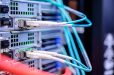
The shift towards these data-intensive and hyper-connected platforms has spurred expanded investments in data centers, enterprise servers, network systems and HPC (high-performance computing) that require the highest level of performance and energy efficiency in large capacities.
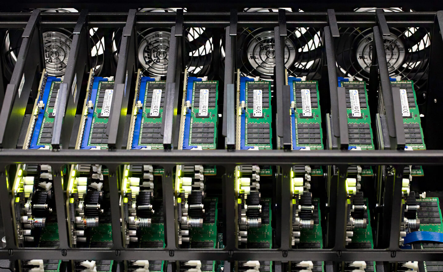
Samsung’s high-capacity memory solutions such as DRAM, V-NAND SSDs and HBM2 (high bandwidth memory) address this growing trend while mobile memory solutions with fast and efficient V-NAND technology continue to power today’s smartphones and tablets.
Samsung image sensors for mobile devices
Along with Samsung’s memory chips, CMOS (complementary metal-oxide-semiconductor) image sensors are also among the S.LSI business’ premium flagship products for Samsung. Its proprietary ISOCELL technology separates each pixel with a physical barrier that hugely boosts image quality and enables smaller pixels.
Consumer demand for Digital Single Reflex (DSLR) quality pictures and dual-lens cameras are spurring growth in the high-performance image sensor market. In addition to image sensors, display driver ICs (DDI), mobile processors and connectivity solutions also add to the business’ comprehensive product portfolio.
Samsung memory business
It all started with the 64Kb DRAM module. About a decade later since its establishment in 1974, Samsung’s semiconductor business made its first mark in the industry with the chip.
Its development narrowed the technology gap with industry forerunners from ten years to four. In 1992, Samsung became the top DRAM manufacturer with the development of the 64Mb DRAM and rose as the top memory manufacturer the year after.
Before there were smartphones, we flipped through phone books to look up a contact person. Just when Samsung’s very first semiconductor was being developed, these company phone books from 1983 and 1984 stored valuable information that connected our organization. Just like the smartphones today, these fit comfortably in the pockets.
Samsung Semiconductor history
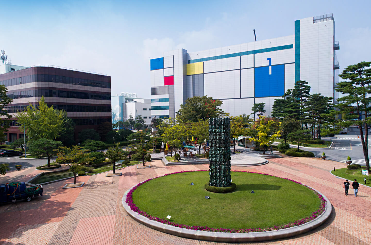
At the heart of the Giheung Campus in Korea is the Administration Building where Samsung’s semiconductor history began in the mid-‘70s. The Admin building and Line 2 stand as they did more than 30 years ago while Line 1 was rebuilt for upgrades.
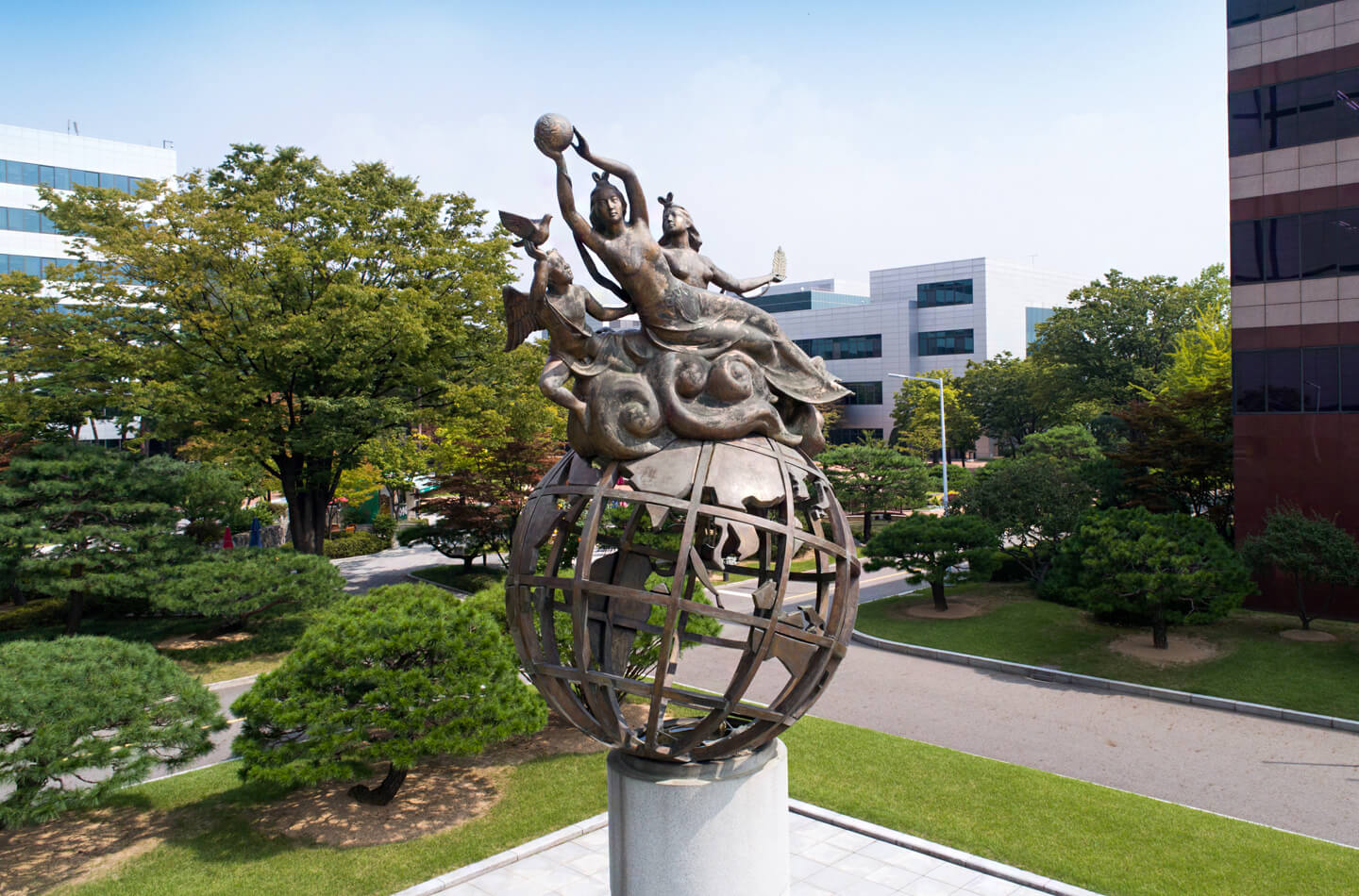
In front of the Administration building stands the Muhantamgusang (Statue of Infinite Study) since Day 1 of Samsung’s semiconductor business. The statue symbolizes founder Byung-chul Lee’s vision and mission for the business, and the spirit of continuous curiosity, research and study is at the core of Samsung’s operations. The bronze statue was commissioned to sculptor Se-Jung Kim, who is famous for his statue of Admiral Yi Sun-sin in Seoul’s Gwanghwamun Plaza.
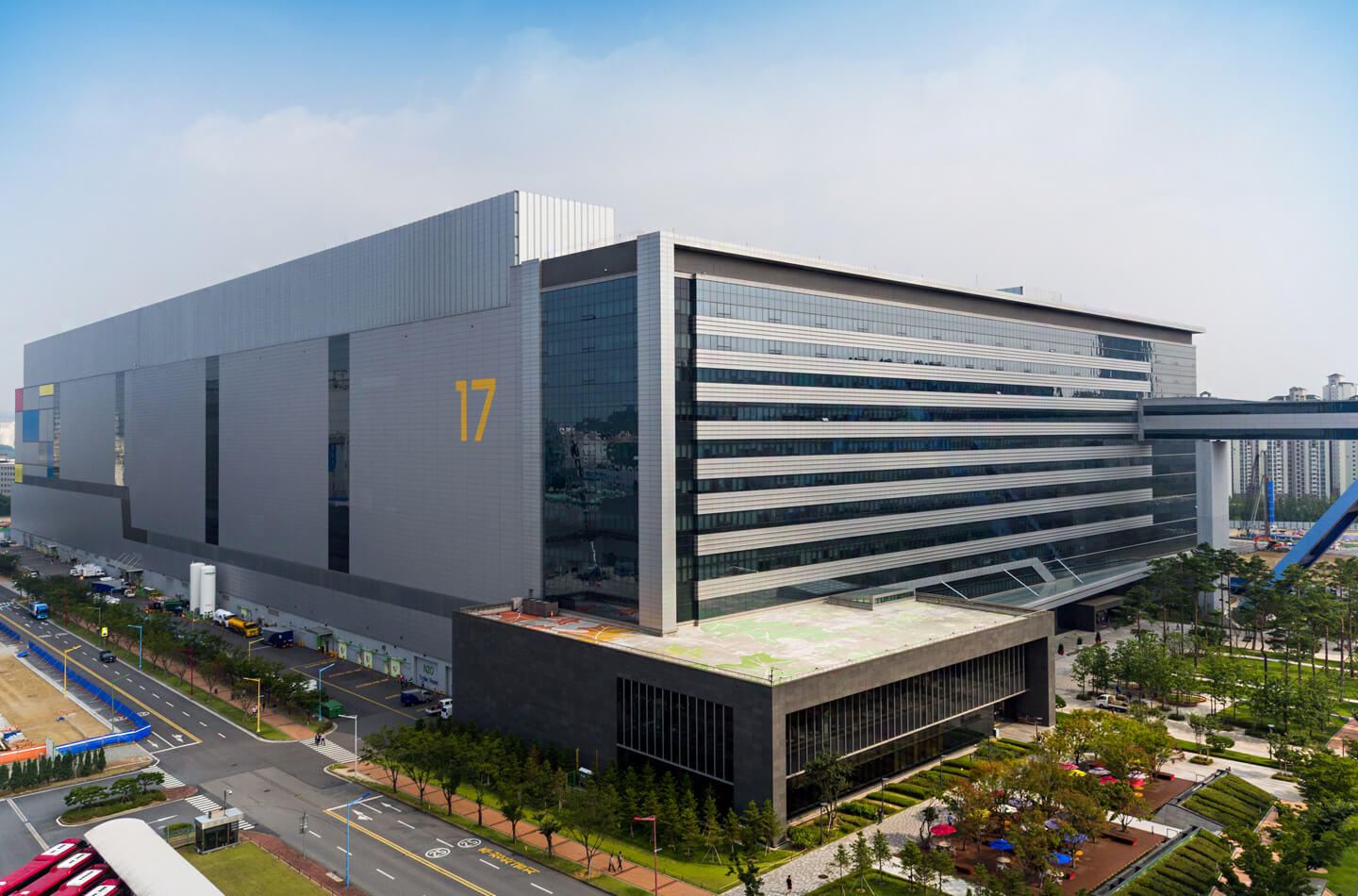
The most recent addition to Samsung’s production lines in Korea is Line 17 in the Hwaseong Campus adjacent to Giheung. Since its opening in 2016, the line has been manufacturing logic chips for foundry customers along with DRAM.
The Foundry Business has successfully been producing the industry’s first 10-nanometer (nm) mobile processor since earlier this year and is diversifying its product lineup to Internet of Things (IoT), automotive parts, home appliances and personal computers.
Semiconductor manufacturing sites
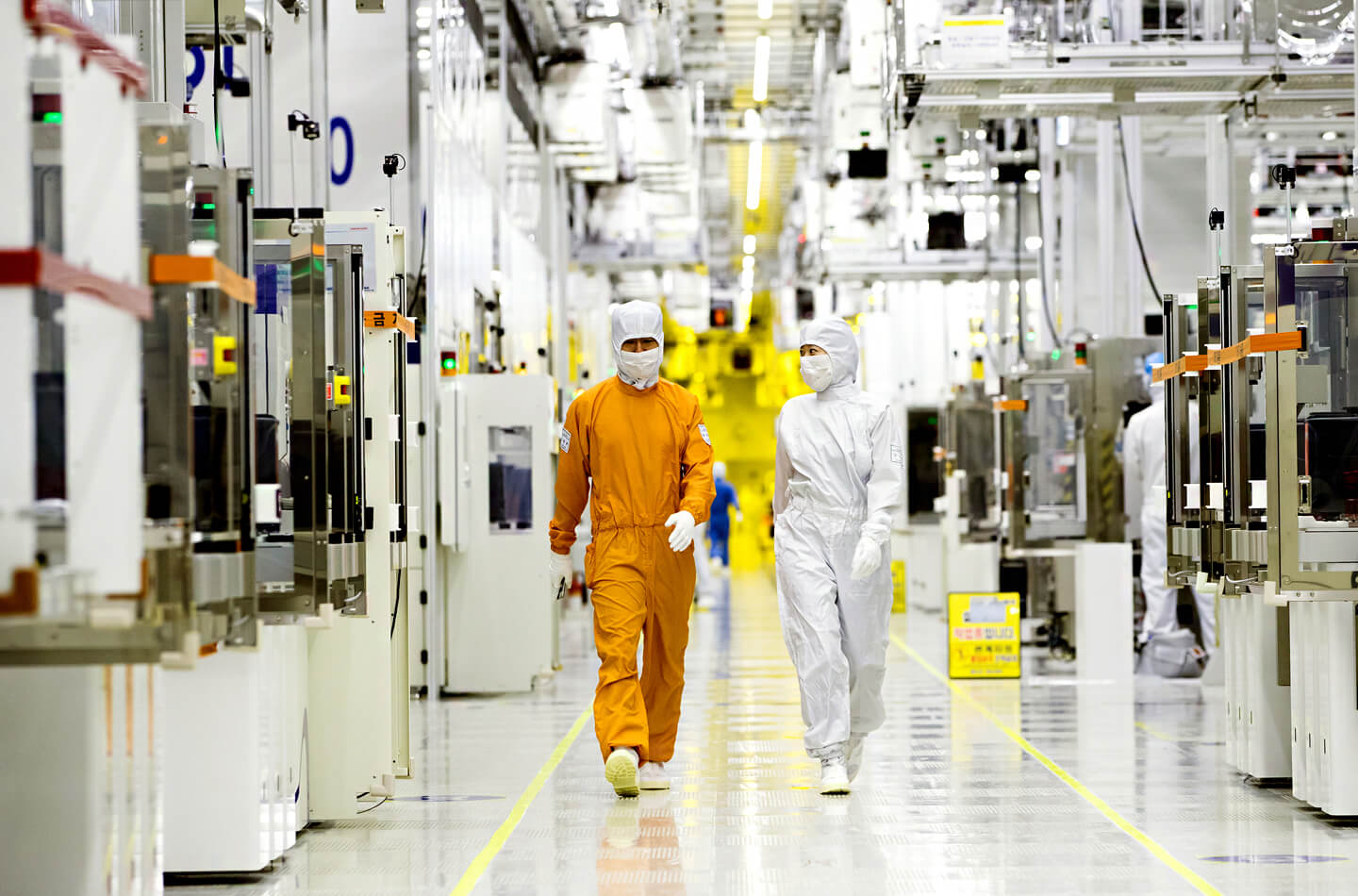
One of the advantages of Samsung’s semiconductor manufacturing sites is that they are in clusters, which allows not only quick decision-making and real-time management around the clock but also tool sharing between manufacturing lines that maximize the efficiency of its resources.
Approximately 23 percent of the industrial water used for Samsung’s semiconductor operations is recycled at wastewater treatment facilities. Internal pollutant discharge standards are set 30 percent lower than the law requires, and discharged water temperatures are strictly controlled to minimize the impact on the ecosystem and redirect the heat for energy reuse.
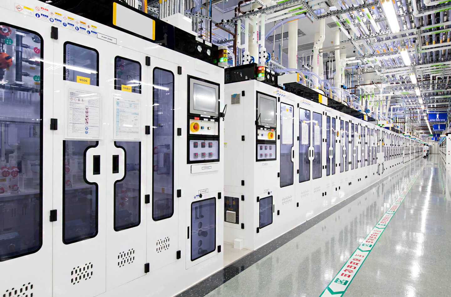
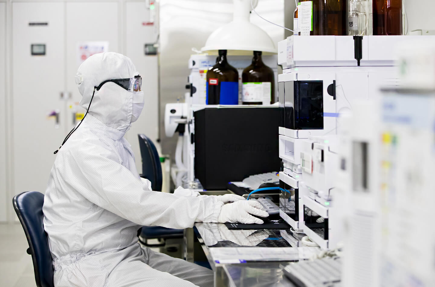
Semiconductor fabrication uses a variety of chemicals in large amounts which demand strict and safe management of these materials. Samsung’s Central Chemical Supply System (CCSS) is where chemicals used in manufacturing are stored and supplied to their destination. Supply systems are enclosed within chambers equipped with local ventilation as a safety precaution.
All piping and joints at the CCSS are doubled and sealed in case of any leakage. The CCSS are monitored 24-7 in real time for chemical input/output as well as any abnormalities such as shortage, leakage or spill.
Samsung Semiconductor technologies
Semiconductor technologies are moving ahead at light speed, but that doesn’t mean that we are exempt from the responsibility to ensure that the technologies and materials we use are safe. Before a new chemical substance is introduced, it is analyzed for physical and chemical characteristics, potential health hazards and any associated risks.
Samsung also established the Health Research Institute, a research organization to safeguard healthy working environments, improve employees’ well-being and raise the standard for assessing workplace health and safety.

Consumer electronics of tomorrow
Semiconductors have been a major precursor to the growth of the IT industry and will continue to inspire innovation in the digital devices of tomorrow.
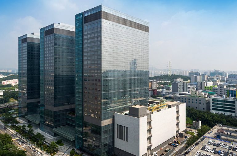
To sustain its edge in the IT landscape, Samsung opened the Device Solutions Research (DSR) center in 2014 to spur collaboration and collective synergy among its semiconductor research and development teams working on numerous projects. The complex is comprised of three 27-story towers and is currently home to more than 10,000 employees.
It is no secret that technological innovation cannot be done alone. The Samsung Research Center (SSRC) within Device Solutions Research (DSR) is an example of Samsung’s collaborative efforts and open partnerships with a wide spectrum of industry innovators.
As we move forward to the fourth industrial wave, Samsung’s semiconductor business continues to push boundaries and looks ahead for the next technological leap that will fundamentally change our way of life and enrich our everyday experiences.
Advertentie